


PCB Layout & Design · ODM PCBA
PCB Layout and Design Services for ODM and Turnkey Electronics
One factory for PCB design, prototyping, PCBA assembly and testing.

- 2006Since
- 220+Staff
- 10,000 m²Facility
- 7SMT Lines
- 2+2DIP / Function Test Lines
Design Decisions Checked by the People Who Build the Board
STHL provides PCB layout and design as part of its ODM PCBA service. Our engineers take your schematic, specification or product idea, lay out the board, review it against our own SMT and testing lines, and move it into prototyping and mass production.

What PCB Layout and Design Services Does STHL Provide?
STHL covers four design tasks. Each can be ordered alone or as part of a full ODM project.
Schematic design
Functional requirements, block diagram, target cost
Schematic, draft BOM, component selection notes
PCB layout
Schematic, BOM, board outline, stack-up requirements
Layout files, Gerber, drill file, BOM, pick-and-place file, assembly drawing
DFM and DFA review
Existing layout or Gerber files
Review report listing required changes and optional improvements
Specialty layout
Interface and impedance requirements, mechanical constraints
Controlled-impedance layout and fabrication notes
How Does STHL's ODM Process Work, From Concept to Mass Production?
ODM (Original Design Manufacturing) means STHL designs the product, or part of it, and builds it. You define the requirements and keep your brand. We take on the engineering and production work.
-
01
Requirement review
We read your specification, target quantity and cost, and list open questions before design starts. Scope, deliverables and milestones are agreed in writing.
-
02
Schematic and component selection
Our engineers select components together with our sourcing team, checking availability, lifecycle status and alternates before the layout is frozen.
-
03
PCB layout and placement review
Layout follows the agreed stack-up and constraints. You review component placement and critical routing before the board is completed.
-
04
DFM, DFA and test-access review
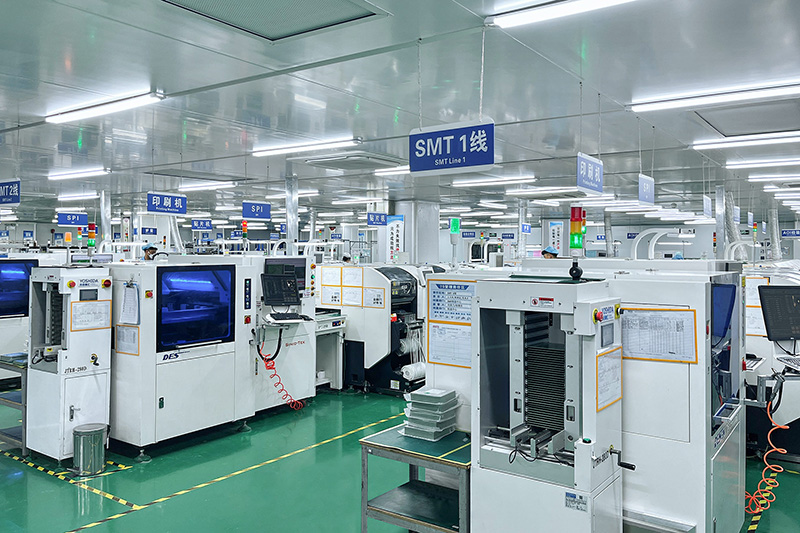
Engineers from our SMT, DIP/THT and testing lines check pad geometry, panelization, assembly clearances and test point access.
-
05
Prototype build and validation
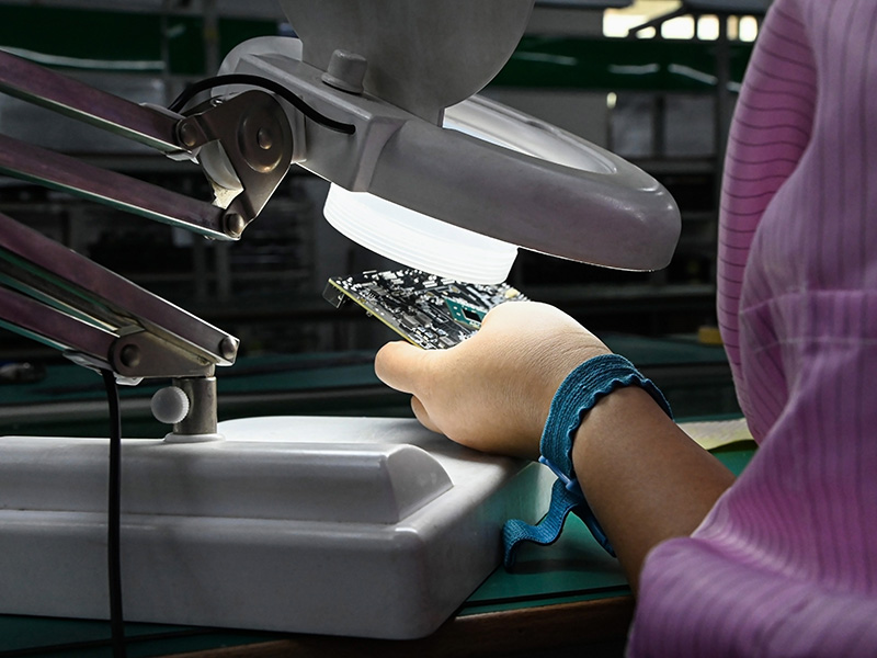
Prototype boards are built on our own lines and checked with AOI, X-ray, ICT and function test. Results go back into the design.
-
06
Release and mass production
The approved package, including Gerber, BOM and assembly files, moves to mass production on the same lines.

| Model | Who designs the board | What STHL does | Typical customer |
|---|---|---|---|
| ODM | STHL, from your requirements | Design, prototype, build and test | Brands and startups without an in-house PCB team |
| Build-to-print (OEM) | You | Manufacture from your complete files | Companies with finished designs |
| DFM review only | You | Review your files and report required changes | Teams about to release a design to production |
Why Does Designing With the Manufacturer Cut Redesign Cycles?
Design choices have manufacturing consequences. When the same company designs and builds the board, those consequences are checked early.
-
Manufacturing feedback arrives before the layout is frozen
Pad shapes, stencil openings and reflow behavior are reviewed by the engineers who run the SMT lines. Assembly problems show up on screen, not on the first prototype.
-
Test access is decided during layout
ICT and function test need probe points and fixture clearances. We place them while routing is still open.
-
Components are checked before routing starts
Our sourcing team reviews availability and lifecycle of key parts, so the design does not depend on a part that cannot be bought.
-
One set of files goes to production
The layout, BOM and assembly files used for prototypes are the files used for mass production.
What Does STHL Need to Quote a PCB Layout Project?
Send what you have. These items let us give you a clear next step faster.
Schematic or functional specification. A block diagram is enough to start.
BOM or a list of key components.
Board outline and mounting constraints (DXF, STEP or a sketch).
Layer count, impedance, material or thickness requirements, if known.
Target quantity, timeline and applicable standards, such as IPC class and RoHS.
If you only have a product idea, send the requirements. We scope the project with you first.
Which Customers and Industries Does This Service Fit?
STHL builds electronics for energy power, communications, automotive, medical, consumer electronics, computers and storage, safety and security, commercial and industrial products. The ODM service fits:
- Hardware startups moving from prototype to production.
- Design houses that need a manufacturing partner.
- Brands and OEMs without an in-house PCB design team.
- Teams redesigning an existing board for cost, availability or manufacturability.
Not a fit: bare-board orders that need no design or assembly (see our PCB fabrication service).
What Quality Systems and Tests Support the Build?
Production runs under IATF16949, ISO9001, ISO14001 and ISO13485 certified systems and complies with the RoHS standard.
Assembled boards are checked with AOI, X-ray, ICT and function test.
- IATF16949
- ISO9001
- ISO14001
- ISO13485
- RoHS
PCB Layout and ODM FAQs
-
What files do I need to send for a PCB layout quote?
A schematic or functional specification is enough to start. A BOM, board outline and target quantity speed up the quote. We confirm anything missing before work begins.
-
Which design software do you work with?
If you use another tool, tell us and we will confirm compatibility before you commit.
-
Does a passed DRC mean the board will work?
No. DRC checks the layout against the rules set for it, such as spacing and clearances. It does not verify circuit function. That is why we add DFM review and prototype testing before release.
-
Can you also manufacture and assemble the board you design?
Yes. PCB fabrication, components sourcing, PCBA assembly, box build and testing are handled in the same factory, using the same design files.
-
Is firmware or enclosure design included?
Scope is agreed in writing before work starts. Tell us if you need firmware or mechanical design, and we will confirm what we can cover.
-
How is my design kept confidential?
Before you send any project files, we will sign a non-disclosure agreement (NDA). We ensure the security of all your project documentation.
-
How long does PCB layout take?
It depends on board complexity, interfaces and the number of review rounds. We give a schedule after reviewing your schematic.
Send Us Your Schematic or Project Brief
Send your schematic or a short project brief to info@sthlpcba.com, or use the form below. Our engineers will reply with scope questions and next steps.
Need assembly only? See our PCBA assembly service.